Australia’s place in the semiconductor world: An introduction to semiconductors
On day one of Australia’s place in the semiconductor world, we present an introduction to the subject, aimed at a reader with no prior knowledge of semiconductors. Below is part one of a four-part feature by Steven Duvall and Glenn Downey.
The purposes of this feature are to broaden and deepen the understanding of semiconductors and their significance for our economy, jobs, productivity and security, and to identify and describe significant roles that Australia could play in the global semiconductor industry with significant benefit to the nation’s economy, jobs, productivity and security.
The feature is organised in four parts.
Part 1 provides background on semiconductors, aimed at an audience with little or no background in the subject, and sets the stage for later parts.
Part 2 describes the impact of recent “chip shortages” and the responses taken by various countries around the world.
Part 3 discusses the significance of semiconductors for Australia.
Part 4 presents a roadmap to help guide Australia’s growth into a significant player in the global semiconductor industry.
1) Semiconductors as materials
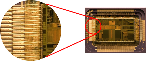
Figure 3 Inside the package of an Intel 80486 (By Matt Britt at the English-language Wikipedia, CC BY-SA 3.0, https://commons.wikimedia.org/w/index.php?curid=5820383)
From everyday experience, we know that different materials vary widely in their electrical conductivity. We know that “conductors,” such as copper and aluminium, readily conduct electricity and are widely used, for example, in wires to distribute electricity. Conversely, we know that “insulators,” such as glass, porcelain and many plastics, are poor conductors of electricity and are widely used to electrically isolate conductors.
Not surprisingly, “semiconductor” materials are in-between, with electrical conductivity intermediate between conductors and insulators. Generally, the term “semiconductor” refers to materials such as silicon, germanium, gallium-arsenide and indium-phosphide that are solid, crystalline and inorganic. (By “crystalline,” we mean materials in which the atoms are arranged in a highly ordered microscopic structure, as shown in Figure 1.) However, the term “semiconductor” can also refer to other materials, including
- amorphous and semi-crystalline inorganic materials, such as polycrystalline silicon,
- certain organic materials, such as semiconductor polymers, and
- liquid semiconductors.
For the most part, we will use the term to refer to solid, crystalline inorganic materials in this article.
Semiconductors are of profound electrical importance because their conductivity can be varied precisely by design. Commonly, very small amounts of other materials, called “impurities” or “dopants,” introduced during the semiconductor device fabrication process (see Section 4) significantly change the electrical conductivity of semiconductor materials. Perhaps less commonly, the conditions under which semiconductor materials are formed determine the crystal orientation and composition of the materials, determining the electrical conductivity.
Importantly, the electrical conductivity of semiconductors can be varied easily and routinely in operation by applying a voltage across the material. This property is fundamental to the operation of the most widely used electronic device made from semiconductor materials, the MOSFET (Metal-Oxide-Semiconductor Field-Effect Transistor). Thus, a voltage applied to the insulated gate of a MOSFET determines the conductivity of the transistor, switching it between a non-conductive “off” state and a conductive “on” state, corresponding to the “0” and “1” states in digital logic.
The most common semiconductor material, silicon, consists of a regular arrangement of silicon atoms in a crystal lattice as shown in Figure 1. Commonly, impurities such as phosphorous, arsenic and boron are introduced into the silicon lattice to change the conductivity and electrical polarity of the material. Thus, silicon can be made n-type (negative electrical polarity with an excess of negatively charged electrons) by the introduction of arsenic or phosphorous and p-type (positive electrical polarity with an excess of positively charged holes) by the introduction of boron.
Silicon dominates the industry due to:
- A significant cost advantage over other semiconductor materials due to the natural abundance of silicon, a mature supply chain, a huge installed manufacturing base and certain physical properties that simplify manufacturing, and
- Significant technical advantages in some applications due to intrinsic properties, including ease of introducing impurities, a high-quality native oxide, purity of the material and the high levels of integration achievable with silicon.
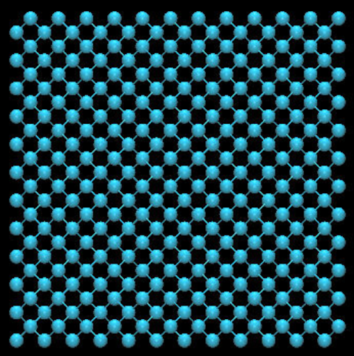
Figure 1 The crystal structure of silicon (https://nanohub.org/tools/crystal_viewer)
Properties AND Performance
For over 50 years, Silicon has been the “best” solution for logic and memory products and “good enough” for many other products. Indeed, over 95 per cent of semiconductor components are currently manufactured using silicon.
However, the properties of silicon are not “good enough” for the performance required of semiconductor components in a broad range of significant applications, most importantly in power management, radio frequency communications and photonics. This has driven the research, development and commercialisation of non-silicon semiconductor materials, including:
- Gallium-arsenide (GaAs), which enabled the multi-billion dollar optical and wireless network industries;
- Indium-gallium-nitride (InGaN), which enabled the multi-billion-dollar solid-state lighting industry; and,
- Gallium-nitride (GaN) and Silicon-carbide (SiC), which are transforming power electronics and radio frequency communications by enabling smaller, lighter and more energy efficient electronic systems.
Most commercially significant non-silicon semiconductor materials are compound semiconductors. In contrast to elemental semiconductors, such as silicon and germanium, compound semiconductors are formed from two or more elements. Thus, GaAs consists of gallium and arsenic atoms arranged in a crystal lattice as shown in Figure 2. Significantly, the electrical, optical and mechanical properties of compound semiconductors can be changed by changing the relative proportions of the individual elements. For example, the wavelength of light emitted from an InGaN light emitting diode can be changed from blue to green or violet by changing the relative amounts of indium (In) and gallium (Ga) in the lattice.
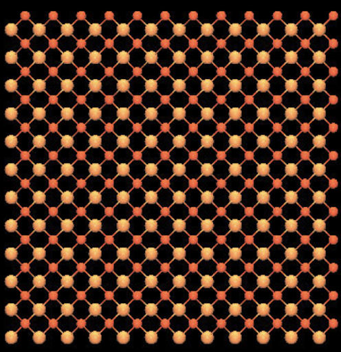 Figure 2 Gallium arsenide crystal structure (https://nanohub.org/tools/crystal_viewer/)
2) Semiconductors as products
Somewhat confusingly, the term “semiconductor” is used not only to describe materials. It is also used to describe electronic components that incorporate semiconductor materials. For clarity, we will refer to semiconductor products as “components” to distinguish them from semiconductor materials. Semiconductor components are also called “integrated circuits,” “microchips” and “microelectronics.” Semiconductor components rely on the physical (electrical, optical and mechanical) properties of semiconductor materials for their functions.
A semiconductor component consists of one or more “chips” (also called “die”) affixed within a “package” and electrically connected to the package. As an example, Figure 3 shows an Intel 80486 chip affixed within a package and electrically connected via wires to metal contacts in the package.
Figure 3 Inside the package of an Intel 80486 (By Matt Britt at the English-language Wikipedia, CC BY-SA 3.0, https://commons.wikimedia.org/w/index.php?curid=5820383)
The chips, which incorporate the semiconductor material, as described in Section 4, deliver the electronic, photonic and other functionality of semiconductor components. The package protects the chips and connects them electrically and thermally to the outside world. Each chip can consist of a single, discrete electronic device, such as a transistor or diode, or it can consist of many electronic devices wired together, forming an “integrated circuit.”
Semiconductor components are essential to virtually every electronic system in use today, including those used in communications, health care, computing, transportation, energy generation and energy distribution, among many other applications.
Semiconductor components are highly diverse in their functions, spanning (electrically) simple diodes and resistors to highly complex microprocessors consisting of billions of interconnected transistors. Examples of high-volume semiconductor components include:
- Microprocessors,
- Computer memory,
- Light emitting diodes,
- Solar cells, and
- Discrete devices, such as rectifiers and power switches.
To illustrate the diversity of semiconductor components, common mobile phones, such as the Apple iPhone X, contain hundreds of different semiconductor components, Figure 4 highlights semiconductor components on three printed circuit boards from the iPhone X.
![]()
Figure 4 Semiconductor components on three printed circuit boards from an iPhone X (https://www.ifixit.com/Teardown/iPhone+X+Teardown/98975)
3) Semiconductor manufacturing
Semiconductor manufacturing is a highly complex, multi-stage process. As shown in Figure 5, we represent semiconductor component manufacturing in four phases:
- Wafer manufacturing: In which wafers are prepared for chip fabrication,
- Chip fabrication: in which chips are formed in and on wafers,
- Dicing: in which wafers are cut into individual chips, and,
- Assembly: in which chips are affixed and connected electrically to packages.
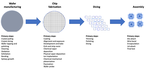 Figure 5 Semiconductor manufacturing flow
3.1 Wafer manufacturing phase
Chips are manufactured in and on flat, disc-like pieces of material, called wafers. Wafers come in a wide variety of materials, sizes and structures, reflecting the wide variety of semiconductor technologies and products in development and use around the world. We will not attempt a comprehensive survey here, but will briefly describe two important types of wafers.
First, most silicon chips are manufactured today on single-crystal silicon wafers sawn from large “ingots” of single-crystal silicon and prepared for chip manufacturing by a sequence of polishing, lapping and cleaning steps. Frequently, one or more thin layers of single-crystal silicon, called “epitaxy layers,” are deposited on the surface of a silicon wafer. Epitaxy layers can deliver significant gains in performance of common silicon semiconductor devices, notably transistors, by enabling the doping to be optimised for device performance or structured to enable more of the device to be formed in high-quality, single-crystal silicon.
Second, most compound semiconductor chips are manufactured on epitaxy wafers, consisting of one or more single crystal layers of compound semiconductor material deposited epitaxially on a wafer that can be of the same semiconductor material as the epitaxy layer or of a different material. Common compound semiconductor wafers include:
- Gallium arsenide wafers used in infrared light-emitting diodes, microwave frequency integrated circuits and photovoltaic cells;
- InGaN epitaxy on sapphire wafers used in blue light emitting diodes for visible light; and,
- Gallium nitride on silicon wafers used in power switching applications.
3.2 Chip fabrication phase
Chips are manufactured on wafers in complex, multi-step processes called “device fabrication,” “wafer fabrication” or “wafer processing.” We will use the phrase “chip fabrication” to distinguish this phase from the first phase, “wafer fabrication,” of the four-phase process in Figure 5 and to avoid confusion about the meaning of a “device.”
As illustrated in more detail Figure 6, in chip fabrication, chips are formed in and on the single-crystal semiconductor layer of the wafer using a complex series of operations. These operations include:
- Additive steps, in which a material is deposited, grown or coated onto the wafer by operations such as physical vapor deposition, chemical vapor deposition and thermal oxidation;
- Removal steps, in which material is removed from the wafer by operations such as etching and chemical-mechanical polishing;
- Patterning steps, in which patterns are formed, most often by selectively exposing and developing a photo-sensitive material on the wafer surface so that portions of underlying layers can be selectively removed or modified; and,
- Modification steps, in which the properties of materials on the wafer are modified by operations such as implantation of impurities and thermal annealing.
The most advanced semiconductor chip manufacturing processes can consist of thousands of individual process steps. At the end of the chip fabrication process, hundreds or thousands of chips have been formed on the wafer.
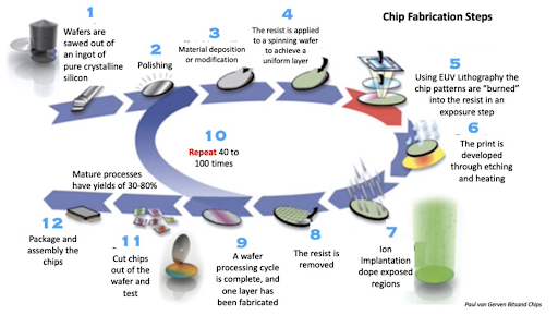 Figure 6 Semiconductor product manufacturing in more detail (https://gordianknot.stanford.edu/sites/g/files/sbiybj22971/files/media/file/The%20Semiconductor%20Ecosystem.pdf)
As illustrated in Figure 7, semiconductor manufacturing is analogous to printing a book.
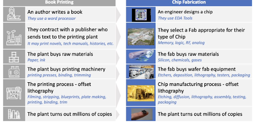 Figure 7 Analogy of semiconductor fabrication to book printing (https://gordianknot.stanford.edu/sites/g/files/sbiybj22971/files/media/file/The%20Semiconductor%20Ecosystem.pdf)
Chips are fabricated in semiconductor fabrication plants, called “Fabs.” Fabs are operated by:
- Integrated Device Manufacturers (IDMs), such as Intel, Samsung and Texas Instruments, that design and fabricate semiconductor components for themselves (and, at times, for others); and by
- Pure-play foundries, such as TSMC and GlobalFoundries, that manufacture semiconductor components under contract to companies that design the semiconductor components.
Pure-play foundries have grown more rapidly than IDMs over the past decade and, in Q3 2022, a pure-play foundry, TSMC, is expected to be the largest semiconductor manufacturer by revenue (https://www.electronicsweekly.com/news/business/tsmc-becomes-no-1-chip-company-2022-09/).
A wide variety of chip fabrication processes are operated in the large number of Fabs operating globally. Chip fabrication processes are distinguished by the types of products (chips) they can produce, the sizes of the wafers they can handle and the minimum feature sizes they can consistently and repeatedly pattern. Thus, different manufacturing processes are used to produce logic, memory, power, RF and analog chips. Wafer sizes from 25 mm to 450 mm diameter can be processed. Minimum feature sizes from 10 microns down to 5 nm can be patterned.
3.3 Dicing phase
In the “Dicing” phase, the wafer can be thinned and polished before it is cut into individual pieces, called chips or die, by a process called “dicing”. Most commonly, wafers are diced by saws or laser scribing and breaking.
3.4 Assembly phase
In the “Assembly” phase, the chips are affixed in packages that provide electrical and thermal contacts. These packaged parts are measured electrically and optically in final test, completing the semiconductor component manufacturing process.
4) The status and impact of the semiconductor industry
As electronics have pervaded our lives, communities and industries, the demand for electronic products, and therefore semiconductor components, has increased exponentially. Semiconductor components are everywhere, from computing, communication and consumer products to healthcare, transportation and smart energy systems. Semiconductor components are now viewed by many countries as a ‘critical technology’ in their own right, as their contribution to economies and security grow in significance. As shown in Figure 8, total semiconductor revenue reached over US$500 billion in 2021 and some forecasts are predicting that it will reach over US$1 trillion by the end of the decade.
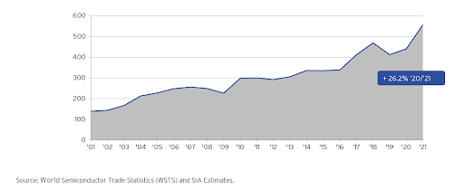 Figure 8 Semiconductor industry revenue growth (https://www.semiconductors.org/wp-content/uploads/2021/09/2021-SIA-State-of-the-Industry-Report.pdf)
The total economic impact of the semiconductor industry far exceeds the revenue generated. As shown in Figure 9, the total economic impact has been estimated to exceed US$7 trillion, with a US$2.7 trillion contribution to global GDP.
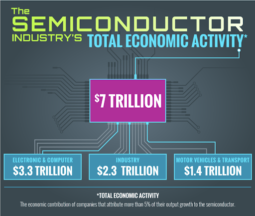 Figure 9 Total economic activity of the semiconductor industry (http://www.semismatter.com/why/)
Most sectors of the economy rely heavily on semiconductors, with the reliance growing with automation, interconnectedness, electrification and communication. Furthermore, as shown in Figure 10, semiconductors underlie most emerging technologies.
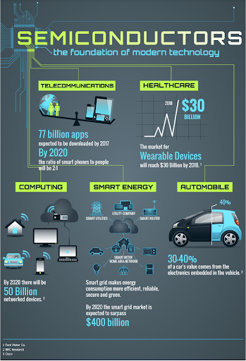 Figure 10 The role of semiconductors in other technologies (http://www.semismatter.com/why/)
As shown in Figure 11, each job in the U.S. semiconductor industry contributes an estimated 5.7 jobs in other parts of the economy.
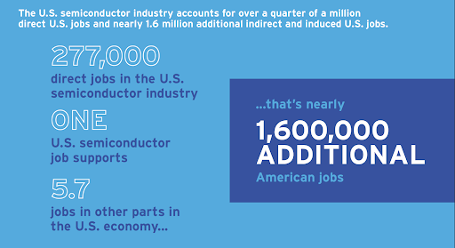 Figure 11 Job creation by the U.S. semiconductor industry (https://www.semiconductors.org/wp-content/uploads/2021/09/2021-SIA-State-of-the-Industry-Report.pdf)
As explained by Steve Blank (https://steveblank.com/2022/01/25/the-semiconductor-ecosystem/) and summarised in Figure 12, the semiconductor industry has seven different types of companies.
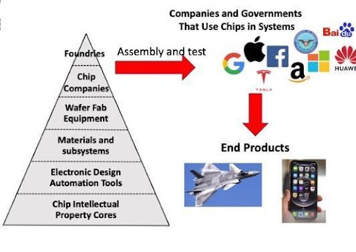
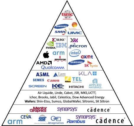 Figure 12 Structure of the semiconductor ecosystem (https://steveblank.com/2022/01/25/the-semiconductor-ecosystem/)
From the bottom of Figure 12, these comprise
- Companies that develop and license “chip intellectual property cores” (IP) include Arm, Rambus and Cadence;
- Companies that develop and sell or license “electronic design automation tools” (EDA) include Mentor Graphics, Synopsys and Cadence;
- Companies that manufacture and sell “materials and subsystems” used in semiconductor manufacturing include Air Liquide, Shin-Etsu and Dow Advanced Energy;
- Companies that manufacture and sell “wafer fab equipment” include ASML, Applied Materials, TEL and Veeco;
- “Fab-less chip companies” that design semiconductor components and outsource manufacturing include Apple, Nvidia, AMD and Qualcomm;
- “Integrated device manufacturers” that design and fabricate semiconductor components, include Intel, Micron and Samsung; and,
- “Foundries” that manufacture semiconductor components for other companies, include TSMC, UMC, Global Foundries and SMIC.
As summarised in Figure 13, semiconductor companies are distributed around the world. The U.S. and Europe lead strongly in R&D intensive activities, including core IP, EDA and manufacturing equipment. Asia leads in capital-intensive activities, including wafer (device) fabrication, assembly, test and packaging.
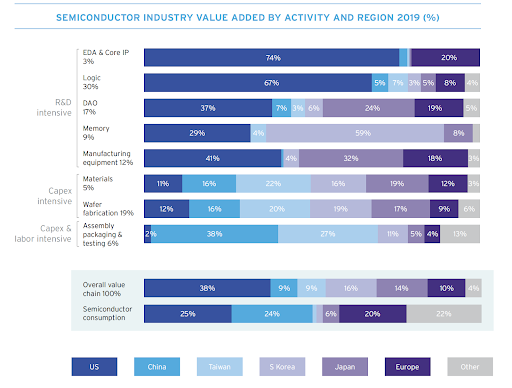 Figure 13 The semiconductor value chain (https://www.semiconductors.org/wp-content/uploads/2021/09/2021-SIA-State-of-the-Industry-Report.pdf)
5) Related technologies
Closely related to semiconductor components are several other product types that are manufactured using similar equipment, processes and manufacturing disciplines. For example,
- Quantum computers rely on semiconductor manufacturing technologies for quantum processors and for the layers of physical interface and processing microelectronics;
- Printed electronics often use processes and technologies closely related to semiconductor manufacturing technologies; and,
- Solar cells are fabricated from silicon and compound semiconductors using manufacturing technologies that are closely related to semiconductor manufacturing technologies.
6) Conclusion
Whether viewed as materials or products, semiconductors are increasingly pervading our lives, enabling modern communication systems, healthcare, transportation and energy generation and distribution. The semiconductor industry continues to grow rapidly, although its characteristic boom- and bust-cycles continue. In part 2 of this series, due to appear tomorrow, we will examine the impacts of recent shortages of semiconductor components, the vulnerabilities they have revealed in global supply chains and the responses they have prompted by countries around the world.
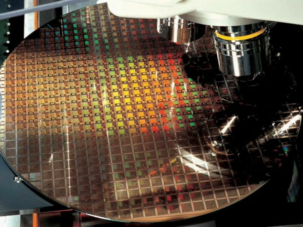
Main picture: TSMC
Dr. Steven Duvall has been in the semiconductor industry for nearly 40 years since completing his PhD at Stanford University in 1983. He spent 18 years with Intel in California driving corporate initiatives in design for manufacturability and six years with Intel in Australia supporting Intel Capital globally with technical and commercial due diligence of entrepreneurial companies. He spent 14 years with Silanna Semiconductor, an Australian developer and manufacturer of advanced semiconductor components, where he was the Chief Technology and General Manager of Ultraviolet Products.
Glenn Downey is Executive Director of The Maltby Group. Glenn was the primary author of the NSW Office of the Chief Scientist and Engineer's ‘Australian Semiconductor Sector Report' (2020). Glenn co-founded and led Sydney based OFDM cable modem technology developer Aurora Communications Limited through till its acquisition by ADC Telecommunications, led the investment and commercialisation activities for Redfern Photonics, the commercialising vehicle for the Australian Photonics CRC, and was Commercialisation Director at NICTA prior to its merger with CSIRO.
@AuManufacturing and AUS-Semiconductor-Community’s editorial series, Australia's place in the semiconductor world, is brought to you with the support of ANFF.

@aumanufacturing Sections
Analysis and Commentary Awards casino reviews Defence Gambling Manufacturing News Online Casino Podcast Technology Videos