BluGlass makes $1.9 million through sale of specialist IP to European company
Semiconductor developer BluGlass has announced a US$1.28 million (approximately $1.93 million) payment from an unnamed European wafer developer for intellectual property rights relating to gallium nitride (GaN) growth techniques on wafers.
According to a statement from BluGlass on Thursday, it developed the specialised IP for the European client under a paid contract development program, which began in January 2022.
BluGlass’s core business is developing and supplying GaN laser diode products to the global photonics industry.
The exclusive IP transfer is limited to Metal Organic Chemical Vapour Deposition (MOCVD) deposition of GaN on the customer’s unique wafer technology. The agreement does not involve transfer of any of BluGlass’s proprietary remote plasma chemical vapour deposition (RPCVD), device, or laser intellectual property.
“The Company’s foundry services leverage our more than a decade of GaN epitaxy expertise to assist in developing next-generation applications,” said BluGlass CEO Jim Haden.
“We’re continuing to support this foundry customer under a paid development contract, with the IP acquisition enabling us to expand our collaboration into a commercial manufacturing contract as the customer’s opportunity matures. Importantly, the transfer of IP applies only to the use of MOCVD GaN growth on the customer’s specialty wafers.”
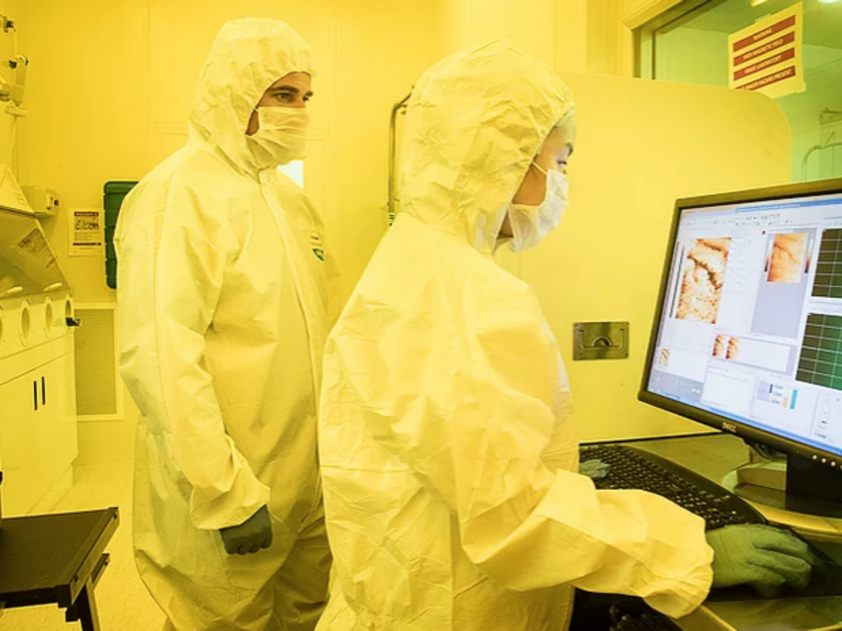
Picture: credit BluGlass
Further reading
BluGlass raises $4.3 million through placement, aims to raise another $9 million through SPP
More in this section


@aumanufacturing Sections
Analysis and Commentary Awards casino reviews Defence Gambling Manufacturing News Online Casino Podcast Technology Videos