@AuManufacturing and AUS-Semiconductor-Community’s editorial series, Australia’s place in the semiconductor world, is brought to you with the support of ANFF.
AuManufacturing
AuManufacturing
Australia’s place in the semiconductor world: Talking about a moonshot
To conclude the second week of Australia’s place in the semiconductor world, we speak to Emeritus Professor Bob Clark about some policy proposals for establishing semiconductor production here, and why this strange era demands we rethink our hands-off approach to the market. By Brent Balinski.
Do we display a lack of ambition in what we might be able to make here?
University of UNSW Emeritus Professor Bob Clark agrees that we do.
“I’m in the category of people that feel that in Australia we’ve lost that manufacturing gene, if you like, that we had,” he tells @AuManufacturing.
“And there’s a tendency – it’s easier to drift towards software, because we all have computers, we can all do various things, including semiconductor design and so on. The really difficult thing is manufacturing.”
Clark recalls the long history of AWA (which spun out its microelectronics division in the 1980s, which evolved into Silanna) and, after an important manufacturing role in World War II, the diminution of its output.
It is difficult – as this series has detailed – but not impossible to make semiconductors here, the topic of our discussion.
Security of semiconductor supply, and appreciation of this, has only grown in importance in this era.
The former prime minister said in March that semiconductors were one of seven areas of manufacturing over which sovereignty was needed and in May tasked Chief Scientist Dr Cathy Foley with developing a national plan for semiconductors.
Since then China’s brazen August military exercises around Taiwan, which produces an estimated 60 per cent of the world’s chips and 90 per cent of its leading edge chips, have only emphasised how fragile the highly-globalised semi industry is.
As for making them here? There is a strong research base, which is an important start.
“When I came back from Oxford in the early 1990s, in the mid-1990s we built a small compound semiconductor [fab] on the ground floor and a silicon CMOS on the upper floor,” Clark says of his time at UNSW, where he established the National Magnet Laboratory and Semiconductor Nanofabrication Facility, and spent two decades leading attempts to build a quantum computer.
“We’re able to put tools into that over the years that took it down to the nanometre-scale where we could actually build nanostructures. And that facility underpinned our quantum computing effort and still does, to this day, in silicon.
“It’s been expanded but largely the guts of that are still functioning and ticking over some 20-odd years later. So we can do this at the research level.”
Making a start with production
Clark is helping answer the question “what does Australia do next?”, through co-authoring (with Alex Capri) a recent Australian Strategic Policy Institute paper, Australia’s semiconductor national moonshot.
“Pragmatically, what can we advise in our humble opinion that might be of help in the somewhat daunting task that Cathy Foley has, as Australian Chief Scientist, of coming up with a national semiconductor plan,” he says of the motivation.

“It’s the most complicated thing you can think of at the really advanced scale, but less so at the mature scale, which is where we think we should go in,” says Clark. (Picture credit: UNSW)
(Foley’s office has not replied to requests for comment for this series.)
Instead of following the argument that Australia has little in the way of semiconductor production here so it shouldn’t start there, it argues the opposite: “Unless Australia makes a start here and addresses this centre of gravity, we’ll forever be a bit player and reliant on foreign supply chains.”
It also acknowledges the nation’s general reluctance to interfere in the market, but contends that intervention is warranted by our extraordinary times.
As Dr Venkata Gutta pointed out yesterday, semiconductor value chains represent the best of global collaboration, due to the highly-specialised goods and services required, though nations are attempting to roll back some of this.
Australia can maybe localise some production, but it’s not going to be creating the most advanced chips, with processes measured in single-digit nanometres.
There are opportunities with mature processes, however, the Moonshot paper points out. The investment required is less eye-watering. Importantly, there are also international markets for chips.
“It’s the most complicated thing you can think of at the really advanced scale, but less so at the mature scale, which is where we think we should go in,” says Clark.
He believes US-based R&D and manufacturing company Skywater, which is making CMOS chips at the “trailing edge” 90-nanometre and 130-nanometre process scales, is notable.
Encouraged by incentives in the CHIPS and FABS Acts in the US, as well as a strong research community at Purdue University (and other factors like the world’s fourth-biggest chip design firm Mediatek nearby), Skywater plans to invest $US 1.8 billion in a semiconductor fabrication facility at Indiana’s Discovery Park District.
Onshoring and friendshoring supply chains
There are customers for trailing edge chips in everything from clean technology to consumer electronics to automobiles. The report points out that the strategic importance of such chips is well known, citing predictions China will go from 15 per cent to 40 per cent of global capacity for 28-nanometre chips by 2025, as well as build 31 fabs by 2024 (compared to 19 by Taiwan and 12 by the US.)
Some experts say there’s a possibility China will retaliate for recent US export controls on advanced chips and related technology by withholding supply of less-advanced chips, which would hold up the global auto market and increase inflation. It would also make sourcing by the US and others from friendly nations more attractive.
“I think people have taken a look and thought ‘we just can’t be reliant on this just in time, global reliance in our supply chains,’” says Clark.
“And we have to probably for the first time in many years think about ‘how do we onshore, friendshore our supply chains in this changing world?’ where I think there are a number of threats that we haven’t had to deal with until quite recently.”
So how should Australia respond?
The paper costs its proposals at $1.5 billion (with an estimated $5 billion in activity created.) These include subsidies and taxes similar to those offered among new US policies, “at say a 30% investment level” to increase the appeal of setting up a fab here, increasing the funding for the Australian National Fabrication Facility (ANFF) by $400 million, and investing the same amount again “to boost an aligned sovereign design capability.”
(Full disclosure: ANFF is the sponsor of this editorial series.)

Picture credit: istock
Compounding the issue
The doubling of ANFF’s budget would raise production to the pilot level “at key nodes”, with the desired effect of attracting public-private investment in a mature CMOS foundry and another in compound semiconductors (CS.)
CS are an area where Australia has acknowledged research strengths
“There are some really important markets there, like the LED market for example,” says Clark.
“It turns out that within the ANFF network there is enormous expertise in compound semiconductors at the R&D level.”
The report notes that the UK has captured a tenth of the fast-growing $US 74 billion CS market, as well as its efforts through the £50 million Catapult program, focussing on markets exploiting the speed, power and light properties of such chips.
Clark speaks favourably of the Australian Semiconductor Sector Study written for the NSW Office of the Chief Scientist & Engineer, though says the ASPI paper differs in its national remit and in considering the role of R&D in growing the sector. The Sector Study does note Australian strength in basic research, but had an acknowledged focus on the commercial side.
Rather than being totally removed from industry, the research community is an important drawcard for private semiconductor businesses and “a critical starting point,” argues Clark.
“Why did [Skywater] go to Purdue in the middle of Indiana? And the answer is that’s where the R&D base is, and the talent pipeline,” he explains, adding that research is not purely the focus, but you’re unlikely to attract private investment without it.
“A commercial entity is not going to invest in Australia in a vacuum. It’s got to link onto something that exists on the ground. And what will be foremost in their mind will be a skilled workforce and a talent pipeline. That doesn’t come from nowhere. It comes from basically an R&D base.”
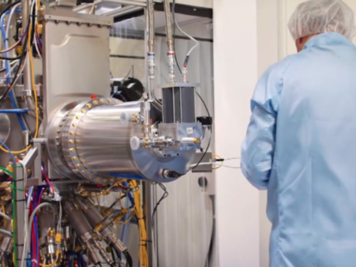
Main picture: Silanna picoFAB Facility at the University of Adelaide (credit University of Adelaide)
Australia's semiconductor national moonshot can be accessed here.
@aumanufacturing Sections
Analysis and Commentary Awards casino reviews Defence Gambling Manufacturing News Online Casino Podcast Technology Videos